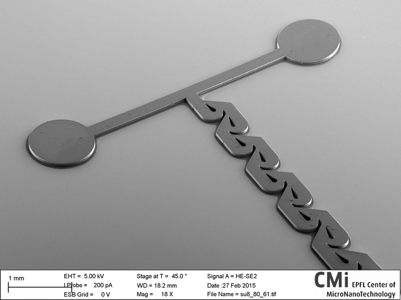
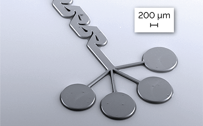
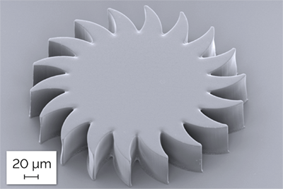
最新桌上型系统µMLA拥有最先进的无掩模直写技术,在进行微结构的研究下,这是一台完美入门级工具;产业领域如微流体、微光学、传感器、微机电和材料科学研究。µMLA具有灵活性以及可制定性,并且能操作毫米等级的示范,有别以往的桌上型无光罩直写解决方案。
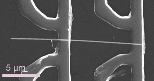
选择您所需要的曝光模式,甚至可为您的µMLA搭配:光栅扫描曝光模块,能快速曝光设计复杂的图形;向量模块,能曝光连续的曲线,创建平滑的轮廓,例如波导的应用。此外,µMLA也提供2种光学配置的选择,在不同的区域产出以及拥有高分辨率。在您的光学配置中,软件也能在三种配置之间转换,并根据您的要求优化分辨率和速度。
NEW: The table-top system µMLA features our state-of-the-art maskless technology and is the perfect entry-level tool for Research & Development, in virtually all areas that require microstructures. Typical examples are Microfluidics, Micro Optics, Sensors, MEMS, and Material Science. The µMLA is flexible and customizable like no other table-top direct writing tool before and supports the use of millimeter-sized samples.
Select the exposure mode you need or even equip your µMLA with both: The Raster Scan Exposure Module provides fast exposure with a speed independent of design complexity. The Vector Module exposes continuous curves, creating smooth contours vital for applications such as waveguides. In addition, the µMLA offers a choice of 2 optical setups with different ranges of throughput and variable resolution. Within your optical setup the software allows easy switching between three configurations, optimizing resolution and speed according to your requirements.
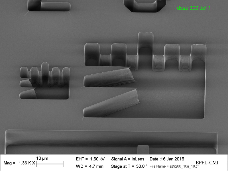
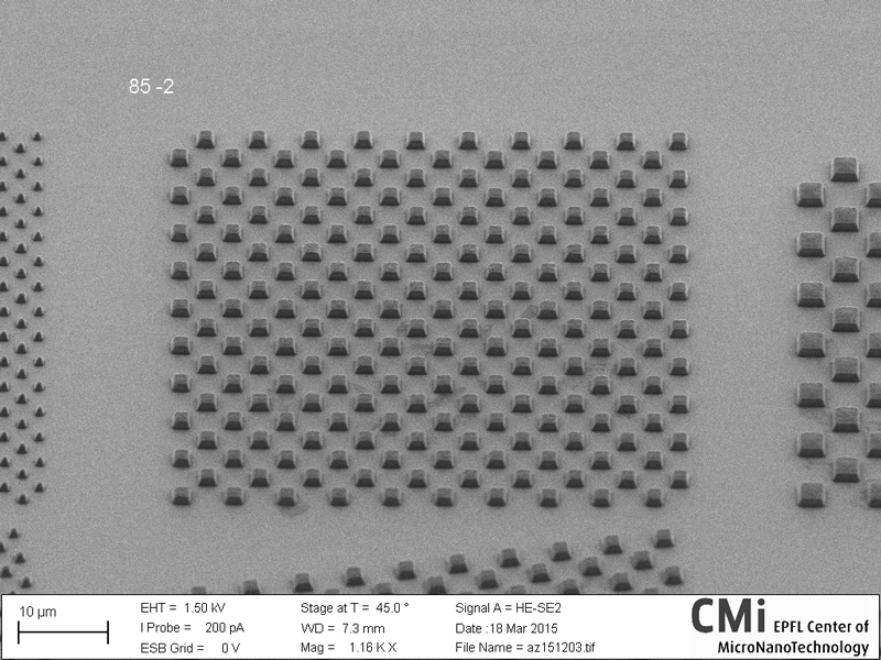
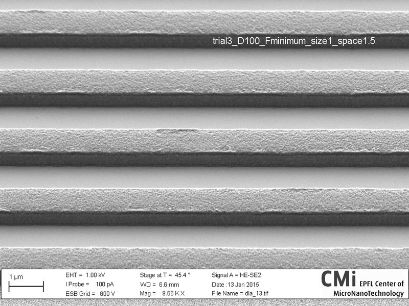
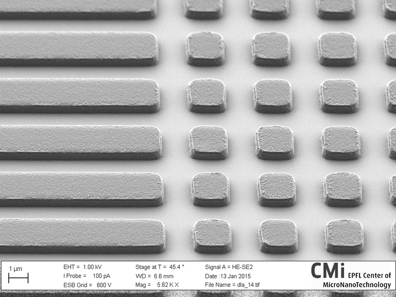
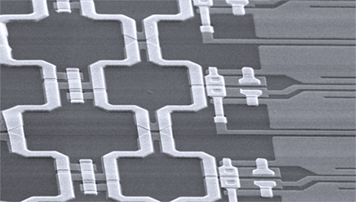
MLA150专为便于操作而设计,涵盖过去30年中开发的激光直写设备的所有技术知识。它提供了单层和多层应用所需的所有功能,由于MLA150曝光是非接触式的,因此它可以克服无掩模曝光技术的局限性。
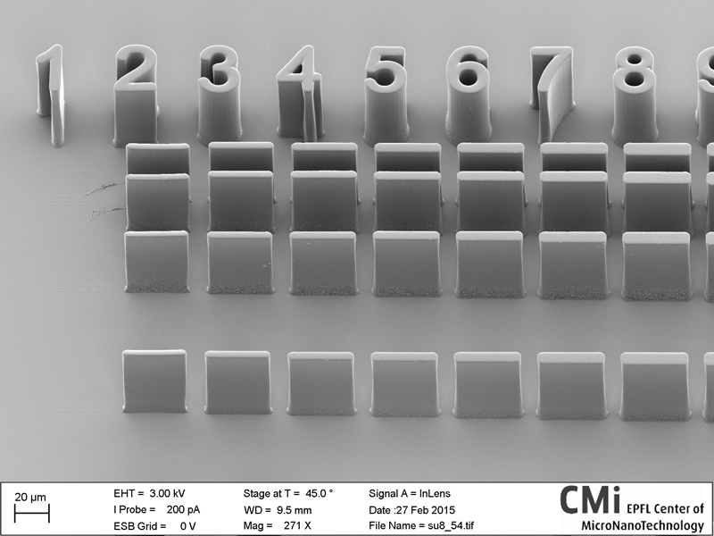
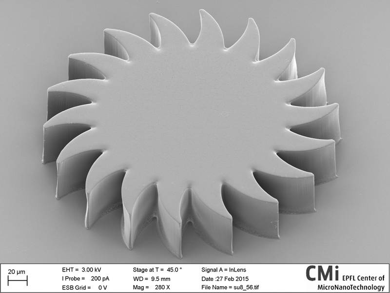
与其他图形产生器不同的地方不仅在于MLA150易于使用,还有极快的曝光速度。使用小至1微米的结构曝光100x100mm²的区域仅需要不到10分钟。透过使用三个不同分辨率的集成摄像头,可在2分钟内完成多层应用中的套刻对位,套刻对准精度优于500nm。
MLA150无光罩激光直写设备直接曝光图形的灵活性能,可提升在Life Science, MEMS, Micro-Optics, Semiconductor, Sensors, Actuators, MOEMS, Material Research, Nano-Tubes, Graphene及任何其他需要微结构等领域的工作效率。
The MLA150 has been specifically designed for easy operation and includes all our know-how on developing maskless lithography systems that we have gathered in the past 30 years. It offers all the capabilities that are required for single layer and multi-layer applications and because the MLA150 exposures are always non-contact it will even overcome some of the limitations of photomask based exposure technologies.
What sets the MLA150 apart from other pattern generators is not only the usability but also the extreme exposure speed. Exposing an area of 100x100mm² with structures as small as 1 micron will take less than 10 minutes – independent of the fill factor or number of structures within this area. Alignment in multi-layer applications is achieved within 2 minutes by using three integrated cameras with varying resolution. Layer to layer alignment accuracy is better than 500nm and does not depend on the operator’s level of training.
Experience the flexibility that the MLA150 Maskless Aligner will provide and expose your layout directly to accelerate your work in the areas of Life Science, MEMS, Micro-Optics, Semiconductor, Sensors, Actuators, MOEMS, Material Research, Nano-Tubes, Graphene, and any other application that requires microstructures.
MLA300是无掩模直写的工业生产版本,能成为研发应用,快速生产以及中小产业量产的标准。 MLA300特色以高生产吞吐量和高可用性,实现2 µm线条和空间的高分辨率。它具有操作晶圆机械手和装载端口的自动化功能,以及针对生产环境设计专门的软件,提供简易操作的自动化工作流程。
同时,也具有光刻直写设备的优点:屏除掩模板采购及处理,清洁和储存的相关开销和费用。
无掩模直写对准技术是使用一种空间光调制器,本质上类似于动态掩模。它灵敏侦测基板上最具挑战性的结构,对每个晶圆进行图案校正(例如,对变形的或工艺变化的产生反应),并采用自动聚焦来跟踪基板的翘曲或起皱。全面性的曝光模块可以选择波长(375 nm或405 nm),依照不同结果作选项;MLA300也可选择安装多组曝光模块,提高吞吐量。
在全球半导体产业中,MLA300运用在IC传感器,微机电设备(MEMS),分立电子组件,仿真和数字IC,集成电路(ASIC),电源电子,OLED显示器以及封装应用的生产领域中都有优秀的表现。
The MLA300 is the industrial production version of the Maskless Aligner, which already has become a standard in Research & Development applications, rapid prototyping, and low-to mid-volume production. The MLA300 achieves high resolutions of 2 µm lines and spaces at the high throughput and high availability expected in production. It features full automation with wafer robot and load ports, and software specifically designed for the production environment to offer a simplified automated workflow.
At the same time, it features all the advantages associated with maskless lithography: Overheads and expense associated with the procurement of masks, and their handling, cleaning, and storage are eliminated.
The Maskless Aligner technology uses a Spatial Light Modulator which essentially acts like a dynamic mask. It offers the flexibility to structure the most challenging substrates, allowing per-die pattern corrections (e.g. to react to distortions or process variations), and employs a real-time autofocus to follow substrate warp or corrugations. The fully integrated exposure modules are available for a selection of wavelengths (375 nm or 405 nm) and with different resolution options. Multiple exposure modules can be mounted in the MLA300 for even higher throughput.
The MLA300 excels in application areas such as the production of sensors, sensor ICs, MEMS devices, discrete electronic components, analog and digital ICs, ASICs, Power electronics, OLED displays, as well as for advanced packaging applications.