热销的VPG(Volume Pattern Generator)系列-全球安装已超过50台。自成立以来,随着技术的进步,VPG产能不断得到进一步提升。整体的高速光学调制器有了飞跃性表现-升级后的系列称之为:VPG+。
VPG+系统同步提供小面积和大面积曝光的设备。VPG+200和VPG+400是海德堡设备中最先进的中小型高速曝光系统,以大面积VPG平台所采用的运作原理,同步保留小面积光刻领域的高端技术。
速度更快:超高速曝光
VPG+系列具有海德堡所研发的高速光学调制器,在速度最大化下,曝光时间可以达到原始VPG的三倍!强化了曝光性能与数据传输路径。
功能和选项:配备性能
VPG+小面积系统采用波长355nm的高功率脉冲紫外激光光源。空气轴承平台能够分别容纳尺寸为200x200mm²或400x400mm²的基板。系统配备自动对准功能和集成计量系统。
应用:掩模制造和直接写入
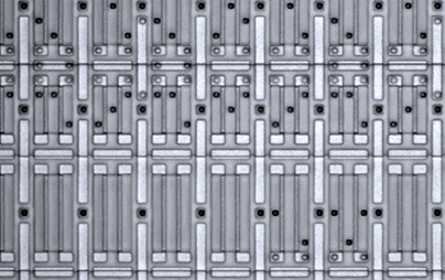
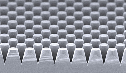
VPG+ 200和VPG+ 400将高分辨率的图像结合优化速度,以达到最快光刻产能,成为光罩制作及其他直写应用的首选设备,特别是使用SU-8或IP 3600等i-line光刻胶的应用。该系统可用于各种要求微观结构的领域,典型应用包括MEMS、advanced packaging、3D integration、LED production、life science和compound semiconductors。
The successful VPG (Volume Pattern Generator) family – with an installation base of more than 50 worldwide – has evolved once more. Since its inception, the VPG product line has continuously been improved further as technology advanced. The newly integrated high-speed spatial light modulator now represents a quantum leap in performance – a development that is reflected in an upgraded product name: VPG+.
The Small Area VPG+: The best of both worlds
Our VPG+ systems are available in versions for small and large area exposures. All of them share the same powerful technology. The VPG+ 200 and VPG+ 400 are Heidelberg Instruments’ most advanced small and midsize high-speed exposure systems. While their principle of operation is based on the technology employed by the company’s large area VPG platforms, they also benefit from our vast experience in small area lithography.
Our Multi-Purpose Volume Pattern Generators are perfectly suited for the production of standard photomasks as well as for i-line resist applications. An ultra-high-speed exposure engine and automated alignment capability both contribute to systems that excel through high resolution, outstanding image quality, and fast throughput.
Our VPG+ 200 and 400 systems present a perfect solution for applications that use i-line resists such as SU-8 and IP 3600, for example for rapid prototyping applications in microfluidics. In combination with their high speed and resolution, the VPG+ 200 and 400 therefore provide an excellent alternative to an i-line stepper.
Typical applications for the smaller exposure area members of the VPG+ family include such demanding fields as MEMS, advanced packaging, 3D integration, LED production, and compound semiconductors.
热销的VPG(Volume Pattern Generator)系列-全球安装已超过50台。自成立以来,随着技术的进步,VPG产能不断得到进一步提升。整体的高速光学调制器有了飞跃性表现-升级后的系列命名为:VPG+。
大光刻面积VPG+:技术的领航
大光刻面积的VPG+维持原VPG系列为根基再进化,使其更加出色。VPG于2007年推出; 是拥有专利的量产型曝光技术光刻系统,可靠和经济的解决方案,适用于要求严谨的掩膜板制造。
速度更快:超高速曝光
VPG+系列具有海德堡所研发的高速光学调制器,在速度最大化下,曝光时间可以达到原始VPG的三倍!强化了曝光动能与数据传输路径。
功能和选项:配备性能
VPG+可配置各种平台尺寸,最大可达1400mmx1400mm。 该系统具有355nm波长的紫外激光源,空气轴承平台,半自动或全自动入料器,用于基板装载和最先进的温控环境室。
应用:掩模制造和直接写入
大光刻面积的VPG+系统适用于advanced packaging, semiconductors, displays, color filters, light emitting diodes, touch panel以及life science应用。出色的图像质量和对位功能,也非常适合在大面积执行多层套刻直写。
VPG+ 最大型的设备VPG+1400专门针对显示器相关行业应用:是所有VPG+系列中功能最强大,具有极其完善的温控环境室,差分干涉仪和先进的mura校正以及面板间距优化功能。
Our Large Area VPG+ systems are perfectly equipped for applications such as photomask fabrication for advanced packaging, semiconductors, displays, color filters, LEDs, and touch panel applications. The systems support all industrial data formats and offer Mura optimization functions ensuring excellent CD uniformity and resolution. The closed-loop environmental chambers comply with the most stringent requirements for use in advanced photomask technology. Because of their speed, attractive system price, and low running costs, the Large Area VPG+ series represents the most productive solution for large area photomask applications.
The VPG+ 1400 is our largest system and particularly aimed at applications in the display industry: FPD applications like TFT-arrays and color filters, and ITO. The VPG+ 1400 features a particularly powerful environmental chamber, a differential interferometer with a resolution down to 1.2 nm, and advanced Mura correction capabilities.
ULTRA特别是针对半导体产业生产掩模板,提供经济量产型的系统。它符合您的需求具有高效产能,高精度和结构均匀性,以及高精确的对准系统。如今当代产业的产能结构密集,需要更快速有效提供您结合现有系统,进而量产的基本配备。
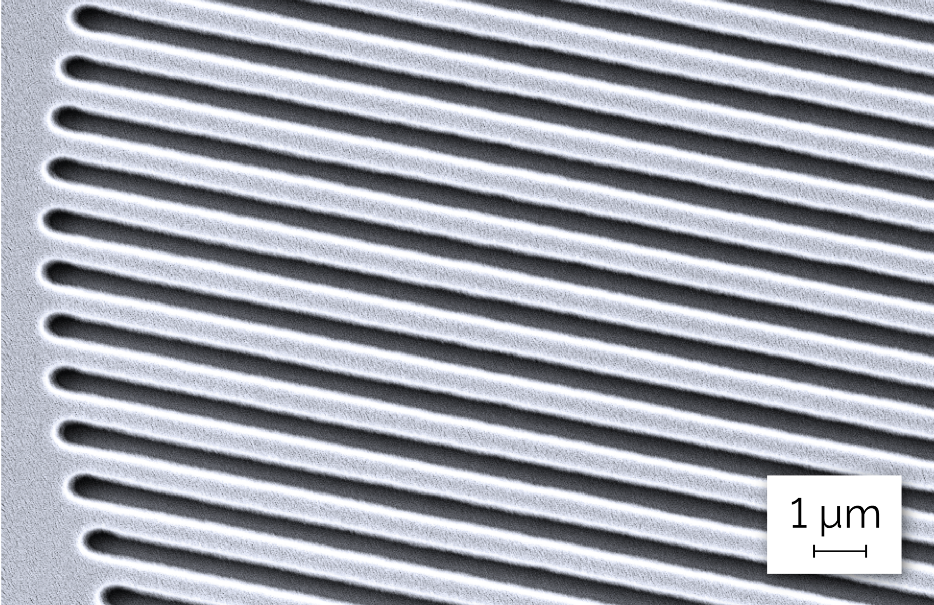
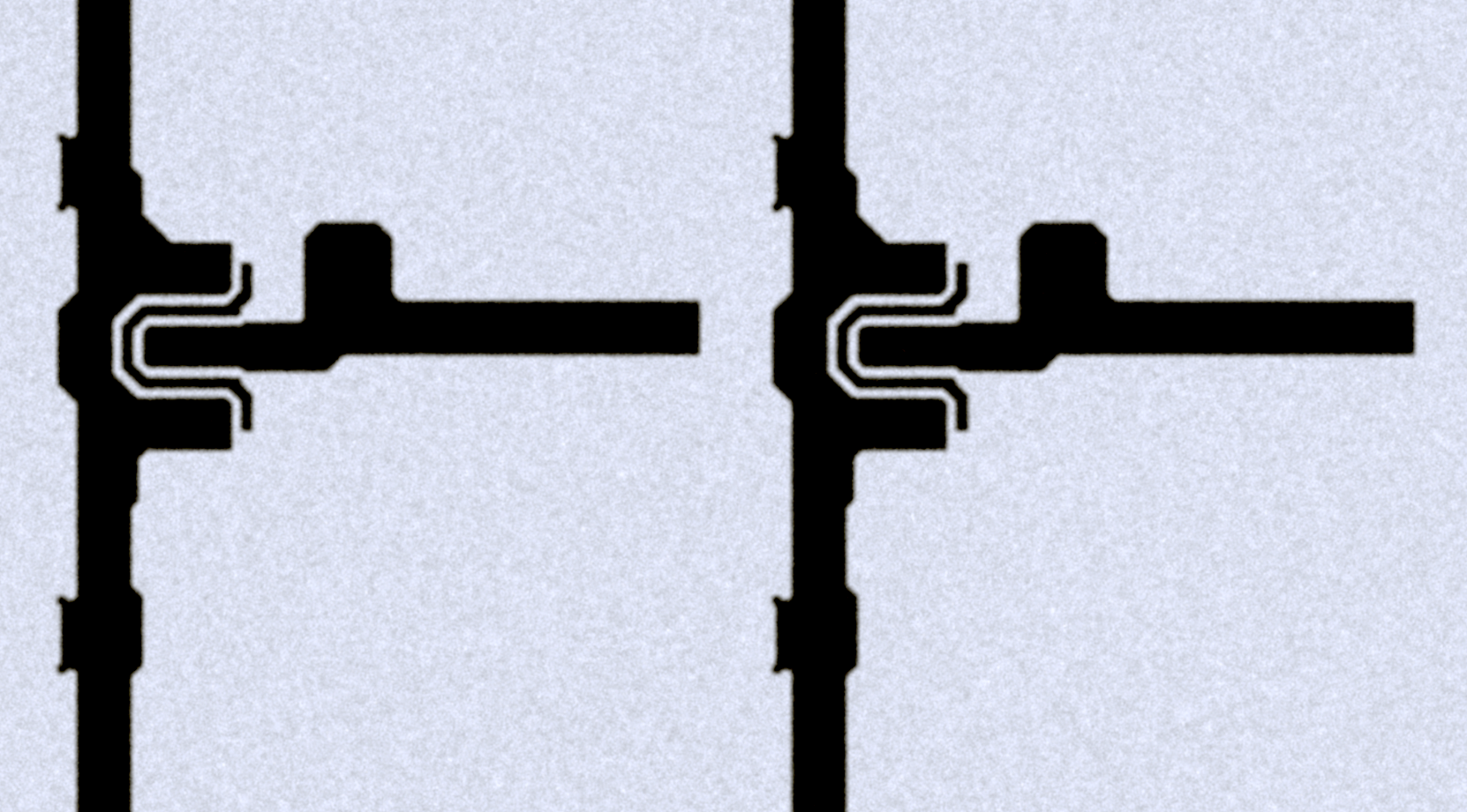
掩模板仍然是半导体器件制造中重要的一部分,用于电源、微控制器、LED照明、物联网、微机电、汽车行业等。ULTRA最小线宽结构可做到500nm,根据写入速度,最快可达每分钟 325mm2或 580mm2,同时具备卓越的CD均匀性、高质量图像、重迭准确和定位值。
The ULTRA specifically addresses the production of mature semiconductor photomasks. It provides an economical mask writer solution with all the features you require for high throughput, high precision and structure uniformity, and extremely accurate alignment. With its modern, compact build, you can easily incorporate the system into an existing mask shop infrastructure.
Mature photomasks continue to be a vital component in semiconductor device fabrication, being used in power management, microcontrollers, LED lighting, the IOT, MEMS, the automotive industry, to name but a few. The ULTRA serves this market with structure sizes down to 500 nm and write speeds up to 325mm² or 580mm² per minute depending on write mode, while featuring excellent values for CD, image quality, overlay, and registration.